Sony and TSMC team up in Japan for the next wave of smartphone imaging
Sony Group and Taiwan Semiconductor Manufacturing Company (TSMC) announced on the 11th that they will establish a joint venture to manufacture next‑generation image sensors, marking a major new chapter for Japan’s high‑end semiconductor ecosystem. The new company will base production at a brand‑new Sony Group factory in Koshi City, Kumamoto Prefecture, with mass production targeted for 2029. The venture will focus on advanced image sensors for smartphones—components that increasingly define camera quality, computational photography, and AI‑driven imaging experiences.
Ownership, scale, and strategic intent
The joint venture will be capitalized at approximately ¥747 billion. Sony Semiconductor Solutions—Sony Group’s semiconductor arm—will hold about 60% and TSMC around 40%, making the JV a consolidated subsidiary of Sony. The move deepens a relationship that the two companies formalized with a strategic basic agreement in May and signals long‑term commitment to pushing the envelope in sensor performance, power efficiency, and manufacturing resilience. While product specifics and capacity targets were not disclosed, the partners’ combined strengths—Sony’s global leadership in CMOS image sensors and TSMC’s advanced process know‑how—position the new entity to set benchmarks for stacked sensor architectures, low‑light performance, and on‑sensor intelligence.
Why Kumamoto matters
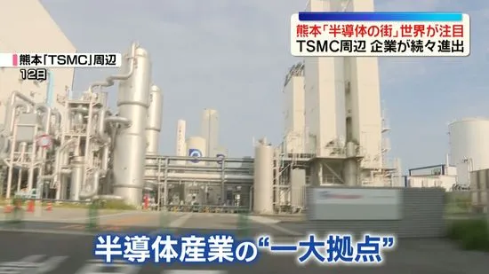
Kumamoto, on Japan’s southern island of Kyushu, has rapidly re‑emerged as a strategic manufacturing hub. TSMC’s entry into the prefecture has already accelerated a broader industrial revival, and Sony’s new factory adds momentum by anchoring a high‑value segment where Japan excels. For Japan, localizing more of the imaging supply chain enhances economic security and reduces logistics risk, while creating skilled jobs and nurturing suppliers in materials, equipment, and precision engineering. The region’s universities and technical colleges are also ramping up talent pipelines, underscoring Japan’s long‑view approach to rebuilding critical semiconductor capabilities.
Technology context: imaging meets AI
Smartphone cameras are now the most‑used cameras in the world, and sensors have become central to device differentiation. Next‑generation image sensors will need to capture more light, render richer color, and interface seamlessly with on‑device AI for features like real‑time scene understanding, low‑noise night shots, and faster autofocus. Sony has led advances such as back‑illuminated and stacked CMOS sensors, while TSMC brings deep expertise in logic processes and advanced packaging—key to bonding sensor and logic layers for speed and efficiency. Together in Japan, the partners can shorten innovation cycles and tighten quality control for global smartphone brands.
Economic impact and opportunities
Beyond technology, the project signals confidence in Japan as a reliable, high‑quality manufacturing base. It supports regional revitalization in Kyushu—historically nicknamed “Silicon Island”—and complements national programs aimed at strengthening advanced manufacturing. For international professionals, Kumamoto’s growing cluster means more opportunities in process engineering, equipment maintenance, materials science, and factory operations. Foreign residents already in Japan—or those considering relocation—will watch closely for recruitment tied to the ramp toward 2029.
Timeline and what to watch
With mass production slated for 2029, the next milestones include factory build‑out, equipment installation, pilot lines, and customer qualification. Market watchers will look for details on sensor architectures, node choices for logic layers, capacity, and sustainability practices. Equally important will be ecosystem development: partnerships with Japanese and global equipment makers, materials suppliers, and local universities to ensure stable operations and continuous innovation. As smartphones integrate more AI features, the Sony‑TSMC JV in Kumamoto could become a cornerstone of the imaging era—delivering better photos for everyday users while elevating Japan’s role in the world’s most competitive consumer technology market.